Our Capability

Precision and Innovation in Every Step

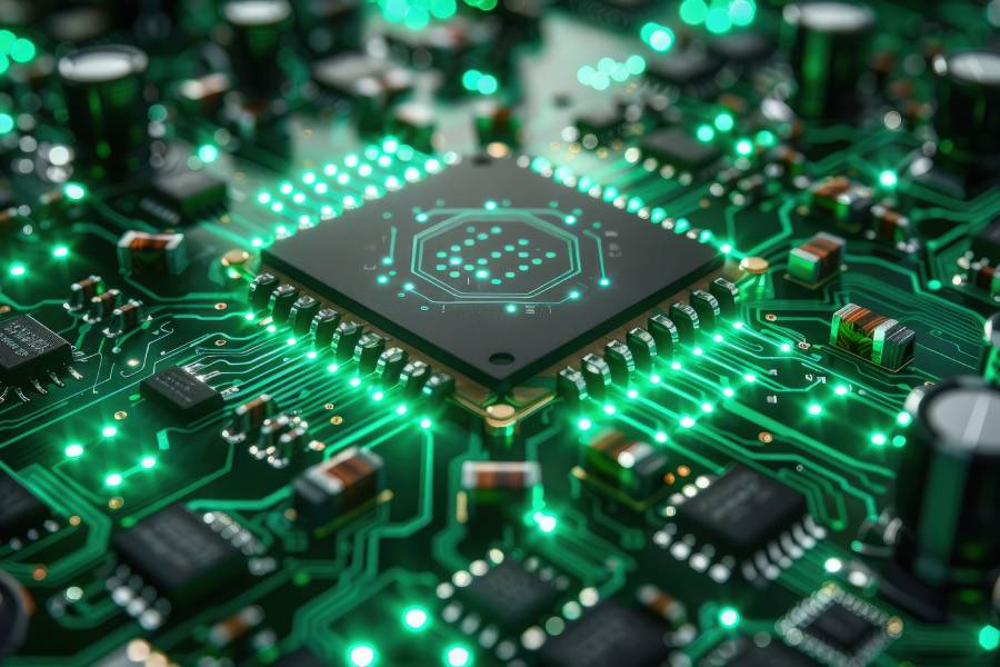
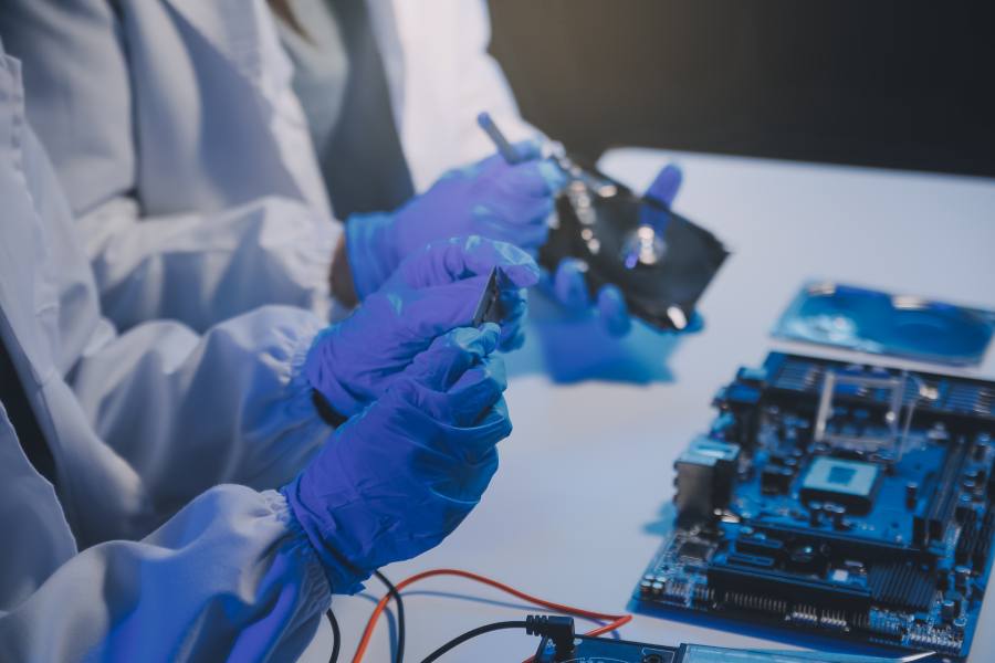
At Quantum Semiconductor Manufacturing Company and Foundries (QSMC Foundries), we take pride in our state-of-the-art manufacturing facility, meticulously designed to deliver unparalleled quality and precision at every stage of semiconductor production. Our advanced processes ensure the highest level of accuracy, from the initial handling of wafers to the final packaging and inspection of semiconductor products.

sqr012-col1
sqr012-col2

Wafer Processing and Handling: Laying the Foundation

Secure Wafer Storage

Incoming wafers are securely stored and meticulously managed to maintain optimal conditions, ensuring they are ready for high-performance processing.

Initial Quality Control

Rigorous testing and inspection of incoming wafers verify their quality and suitability for subsequent steps, ensuring only the best materials are used.

Wafer Taping and UV Curing

To protect wafers during processing, we apply protective tape, followed by UV curing, safeguarding their surfaces for the next steps in manufacturing.

Precision Back Grinding and Polishing

Back grinding and polishing ensure the wafers achieve the perfect thickness and smoothness, a critical step for optimal performance in semiconductor applications.

Dicing and Sawing

We utilize high-precision cutting tools to dice wafers into individual semiconductor chips, setting the stage for packaging and integration.

Die Processing and Attachment: Building Strong Connections

Die Attach and Bonding
Semiconductor dice are securely bonded to their substrates, ensuring robust and reliable electrical connections for maximum performance.
Epoxy Curing
Using advanced epoxy curing techniques, we ensure that the semiconductor dice are securely attached, providing long-term stability and protection.
Wire Bonding and Testing
Fine wires are carefully bonded between the die and external circuitry, with thorough testing of wire strength to ensure the integrity of the connections.
Comprehensive Plasma Cleaning
We use advanced plasma cleaning techniques to remove any contaminants, ensuring a clean, reliable, and high-quality semiconductor product.

Advanced Testing and Inspection: Quality You Can Trust

Optical and X-Ray Inspections

QSMC Foundries employs detailed optical and X-ray inspections at multiple stages to detect any defects or inconsistencies, ensuring that all products meet stringent quality standards.

Die Shear and Cratering Tests

We conduct rigorous tests to evaluate the strength of bonds and assess any potential defects, guaranteeing the reliability and durability of each product.

Semiconductor Packaging: Durability and Protection

Encapsulation and Molding

We encapsulate semiconductor chips in protective molding compounds to shield them from environmental factors and mechanical stress, ensuring long-term durability.

Post-Mold Curing

After molding, the encapsulation material undergoes curing to achieve optimal hardness and stability, enhancing the longevity and protective qualities of the package.

Final Packaging and Shipment: Ensuring Perfection

Laser Marking for Traceability

Precision laser marking ensures that each semiconductor package is identifiable, traceable, and ready for integration into automated systems.

Tape & Reel Packaging

We package units in convenient tape-and-reel formats, ideal for seamless integration into automated assembly lines.

Vacuum Sealed Final Packaging

To protect against moisture, contaminants, and damage, our semiconductor products are vacuum-sealed, ensuring they arrive at their destination in perfect condition.

Innovating Every Step of the Way

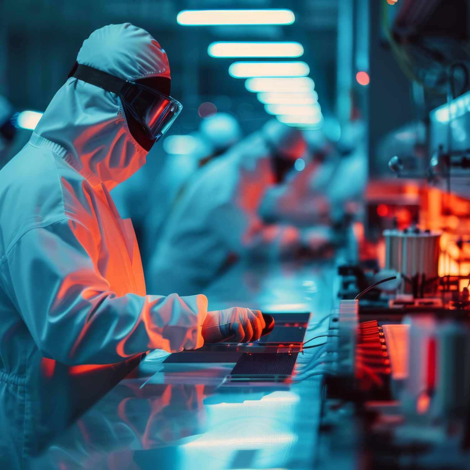
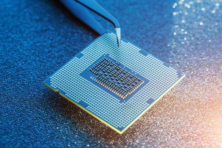
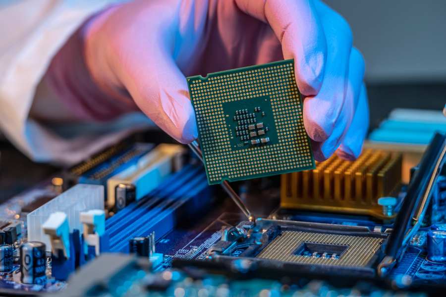
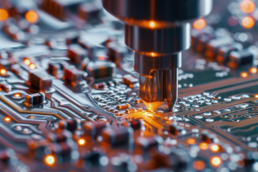
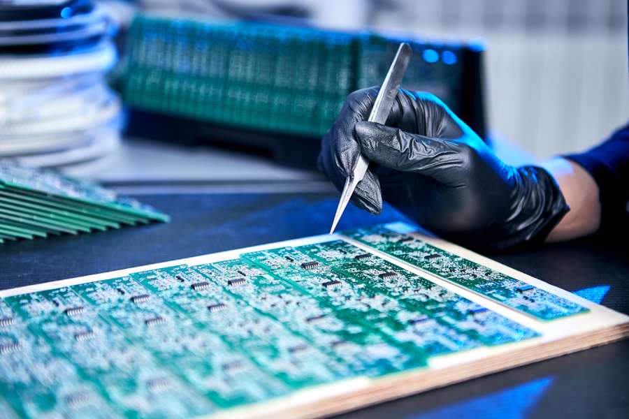
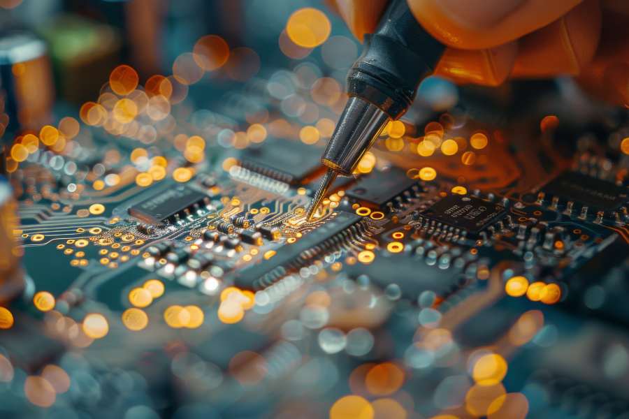
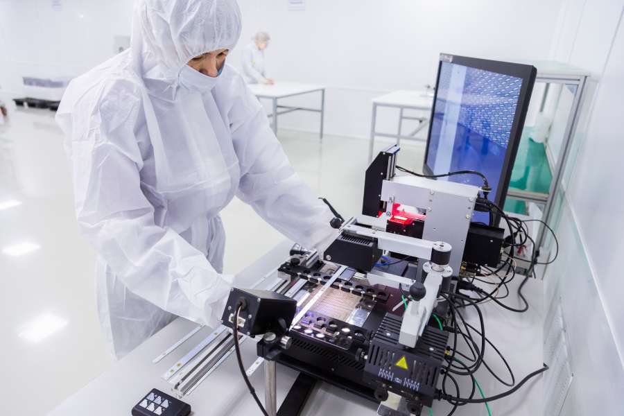
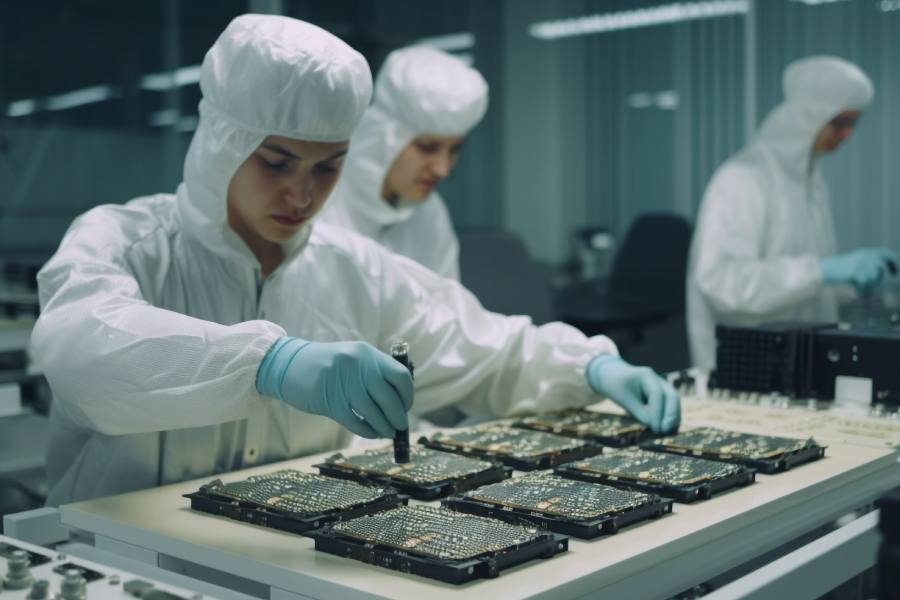
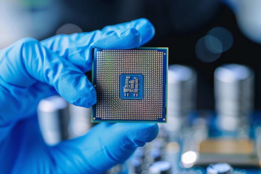
At QSMC Foundries, we are dedicated to driving innovation across every stage of semiconductor production. From wafer processing to final packaging, we ensure precision, reliability, and quality in every chip we create. Our comprehensive capabilities allow us to offer world-class semiconductor solutions that power the technology of tomorrow.

sqr021-col1
sqr021-col2

Automate HR Support With
QSMC